pcb layout design tutorial pcb design steps complete guide complete guide to pcb layout design steps and rules circuit diagram ...
If you are looking for How to Design a PCB easily with EasyEDA & JLCPCB - Complete Tutorial you've visit to the right page. We have 25 Pics about How to Design a PCB easily with EasyEDA & JLCPCB - Complete Tutorial like Complete Guide To PCB Layout Design Steps And Rules – PCB HERO, Complete Guide To PCB Layout Design Steps And Rules – PCB HERO and also PCB Design Tutorial Using EasyEDA & JLCPCB | PCB Designing. Here you go:
How To Design A PCB Easily With EasyEDA & JLCPCB - Complete Tutorial
 www.youtube.com
How to Design a PCB easily with EasyEDA & JLCPCB - Complete Tutorial ...
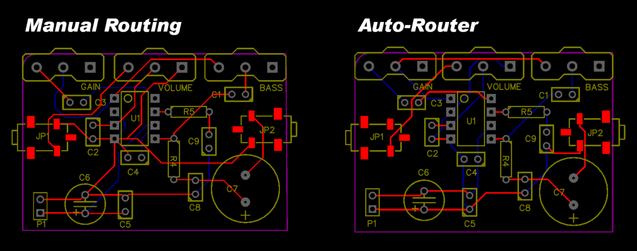
Top 10 PCB Layout Tips For Beginners – PCB HERO
 www.pcb-hero.com
Top 10 PCB Layout Tips for Beginners – PCB HERO
Printed Circuit Board Layout Tutorial - Circuit Diagram
 www.circuitdiagram.co
Printed Circuit Board Layout Tutorial - Circuit Diagram
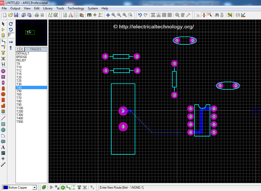
PCB Designing: How To Design A PCB - Step By Step Guide
 www.electricaltechnology.org
PCB Designing: How To Design a PCB - Step by Step Guide
Learn How To Design PCBs With The Best PCB Design Tutorial
 resources.altium.com
Learn How to Design PCBs with the Best PCB Design Tutorial
How To Draw PCB And Design PCB Schematics? – PCB HERO
 www.pcb-hero.com
How To Draw PCB and Design PCB Schematics? – PCB HERO
Complete Guide To PCB Layout Design Steps And Rules Circuit Diagram
 declanstarling.pages.dev
Complete Guide To PCB Layout Design Steps And Rules Circuit Diagram ...
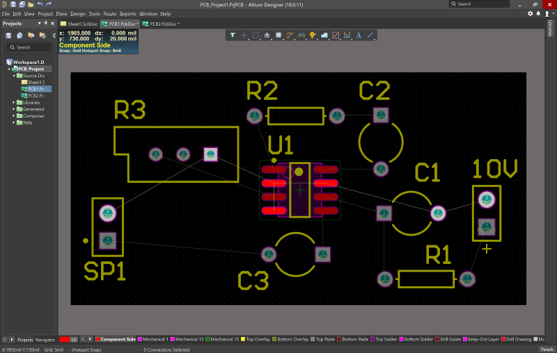
How To Design PCBs Using Altium [Step By Step Altium Tutorial] | RootSaid
![How to Design PCBs using Altium [Step by Step Altium Tutorial] | RootSaid](https://rootsaid.com/wp-content/uploads/2022/06/Altium-Tutorial.png) rootsaid.com
rootsaid.com
How to Design PCBs using Altium [Step by Step Altium Tutorial] | RootSaid
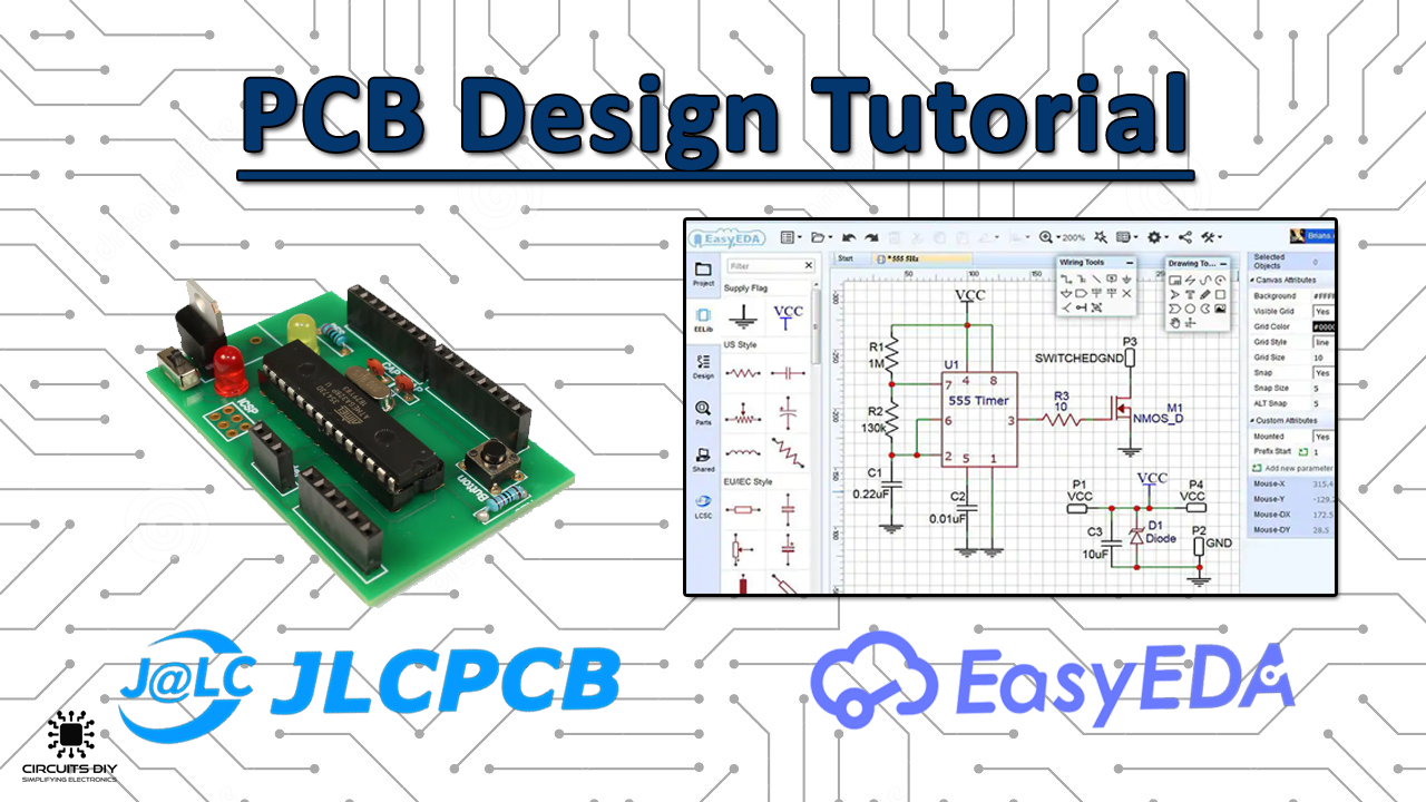
PCB Design Tutorial Using EasyEDA & JLCPCB | PCB Designing
 circuits-diy.com
PCB Design Tutorial Using EasyEDA & JLCPCB | PCB Designing
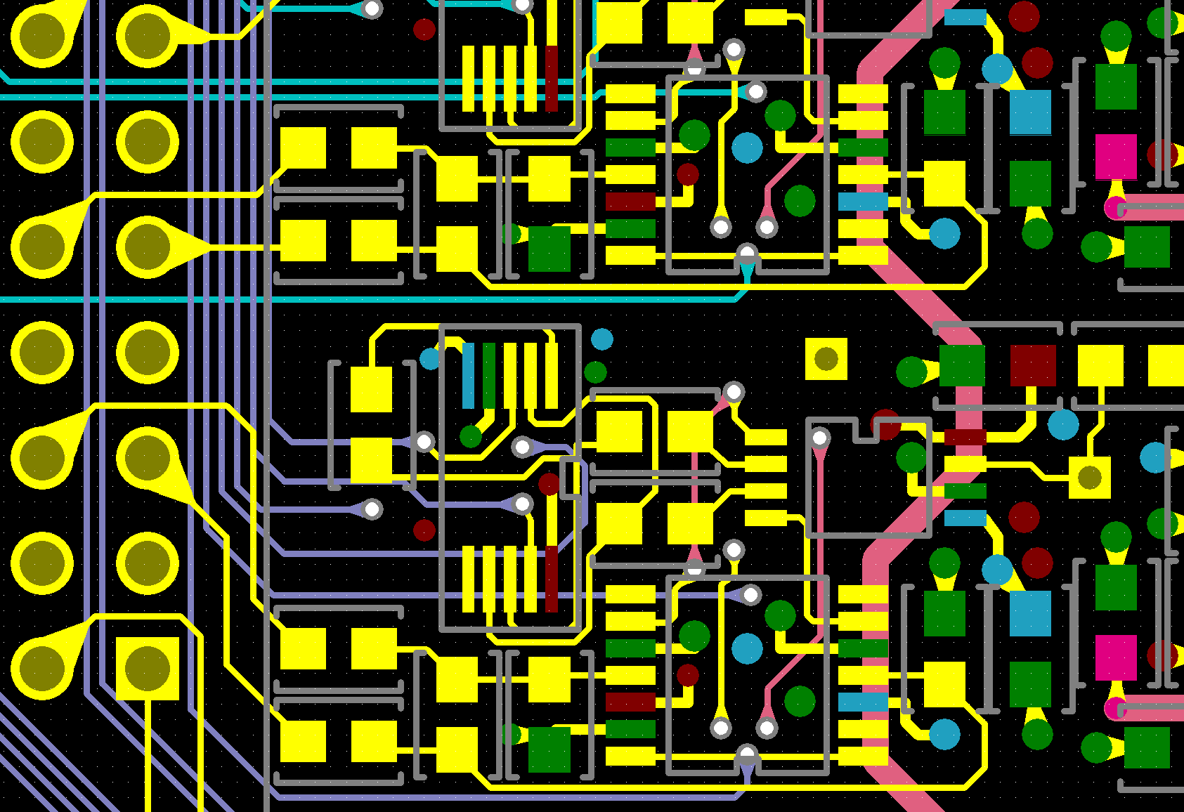
A Complete Guide To PCB Design And Layout - Circuit Basics
 www.circuitbasics.com
A Complete Guide to PCB Design and Layout - Circuit Basics
Quickly Complete Panelization With CAM350 - TechSparks
 www.tech-sparks.com
Quickly Complete Panelization with CAM350 - TechSparks
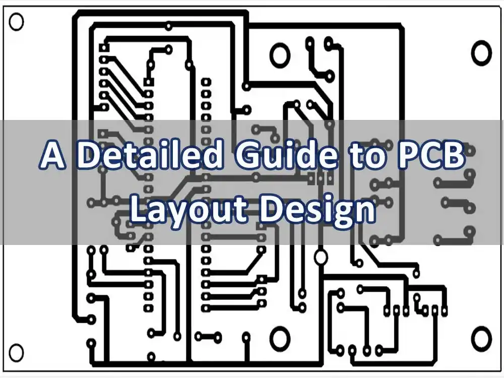
Complete Guide To PCB Layout Design Steps And Rules – PCB HERO
 www.pcb-hero.com
Complete Guide To PCB Layout Design Steps And Rules – PCB HERO
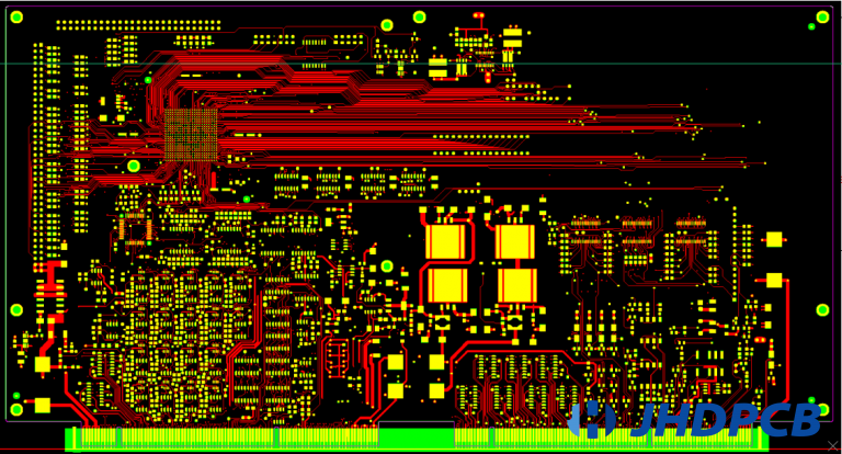
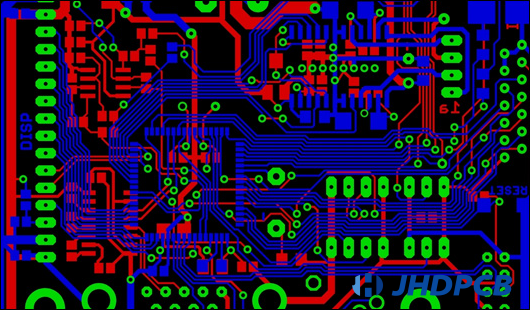
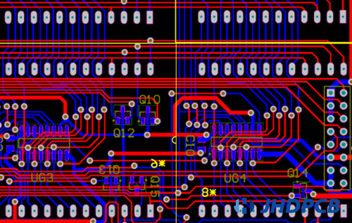
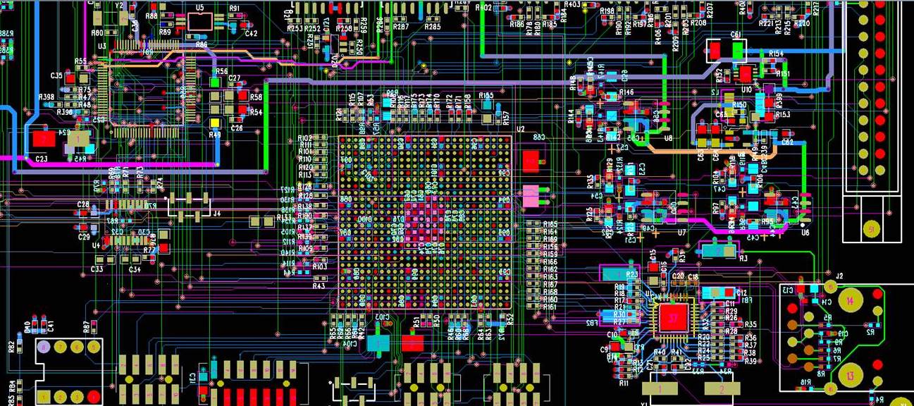
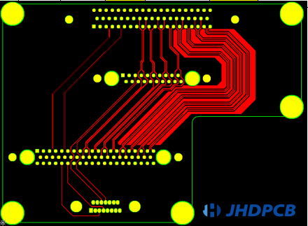
Complete Guide To PCB Layout Design Steps And Rules - Jhdpcb
 jhdpcb.com
Complete Guide To PCB Layout Design Steps And Rules - Jhdpcb
Complete Guide To PCB Layout Design Steps And Rules – PCB HERO
 www.pcb-hero.com
Complete Guide To PCB Layout Design Steps And Rules – PCB HERO
Te Văd Chiriaş Strâmtoarea Bering Generate Pcb From Schematic Stres
 furnituremodern.com
Te văd chiriaş Strâmtoarea Bering generate pcb from schematic stres ...
Pcb Schematic And Layout How To Design A Pcb Layout
 babogediboplibguide.z13.web.core.windows.net
Pcb Schematic And Layout How To Design A Pcb Layout
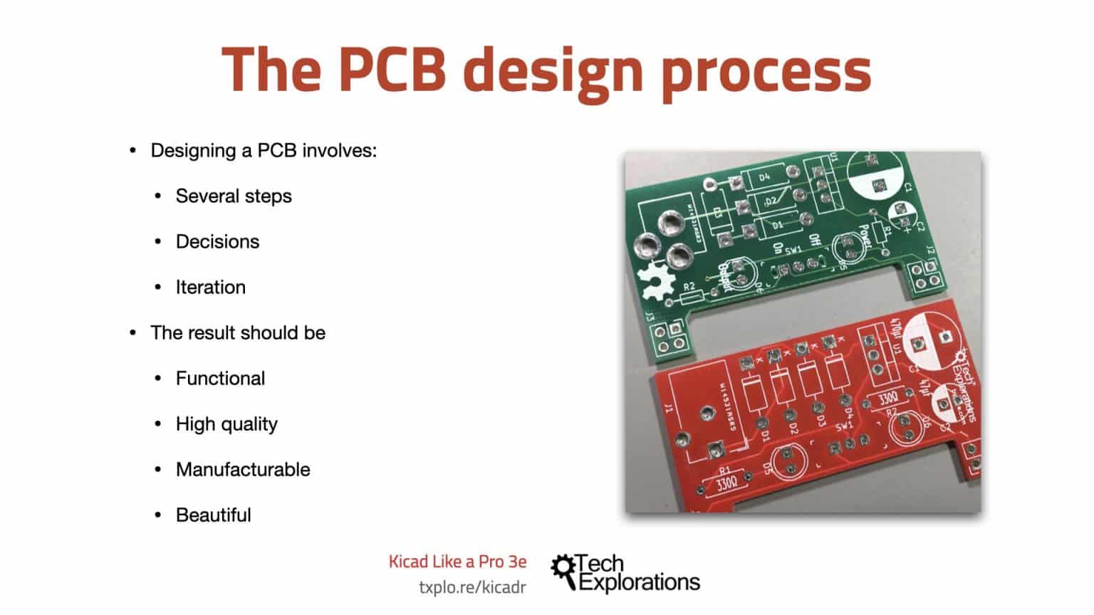
Tech Explorations - KiCad 6 Guide Series - The PCB Design Process
 techexplorations.com
Tech Explorations - KiCad 6 Guide Series - The PCB design process
Complete PCB Design Tutorial [2019] | OrCAD/Allegro 17.2 - YouTube
![Complete PCB Design Tutorial [2019] | OrCAD/Allegro 17.2 - YouTube](https://i.ytimg.com/vi/BTvbXGL6rxE/maxresdefault.jpg) www.youtube.com
www.youtube.com
Complete PCB Design Tutorial [2019] | OrCAD/Allegro 17.2 - YouTube
How To Design A PCB Layout Step By Step? Video+Text-TechSparks
 www.tech-sparks.com
How to Design a PCB Layout Step by Step? Video+Text-TechSparks
PCB Design Steps & Complete Guide | Cirexx
 www.cirexx.com
PCB Design Steps & Complete Guide | Cirexx
PCB Design Steps & Complete Guide - Cirexx | PDF | Printed Circuit
 www.scribd.com
PCB Design Steps & Complete Guide - Cirexx | PDF | Printed Circuit ...
Your Guide To PCB Design Basics & Steps – Hillman Curtis: Printed
 hillmancurtis.com
Your Guide to PCB Design Basics & Steps – Hillman Curtis: Printed ...
Complete Guide To PCB Layout Design Steps And Rules - Jhdpcb
 jhdpcb.com
Complete Guide To PCB Layout Design Steps And Rules - Jhdpcb
Your Guide To PCB Design Basics & Steps
 hillmancurtis.com
Your Guide to PCB Design Basics & Steps
Complete Guide To PCB Layout Design Steps And Rules Circuit Diagram
 declanstarling.pages.dev
Complete Guide To PCB Layout Design Steps And Rules Circuit Diagram ...
Pcb design tutorial using easyeda & jlcpcb. pcb schematic and layout how to design a pcb layout. Pcb design steps & complete guide